Products You May Like
A newly developed transistor device has shown exceptional levels of resilience in tests, performing so well, in fact, that it promises to transform the electronics and gadgets we make use of each day.
These tiny toggles are essential in just about every modern day electronic device, involved in storing data and processing information in a binary ‘on’ or ‘off’ state, switching back and forth multiple times a second.
Thanks to its remarkable combination of speed, size, and resilience to wear, this latest design potentially represents a huge upgrade for consumer devices like phones and laptops, as well as the data centers that store all of our information in the cloud.
Our machines and systems could get significantly faster and more efficient as well as more robust, according to the international team of researchers behind the new study, if the technology can be scaled up to practical levels.
“In my lab we primarily do fundamental physics,” says physicist Pablo Jarillo-Herrero from the Massachusetts Institute of Technology (MIT).
“This is one of the first, and perhaps most dramatic, examples of how very basic science has led to something that could have a major impact on applications.”

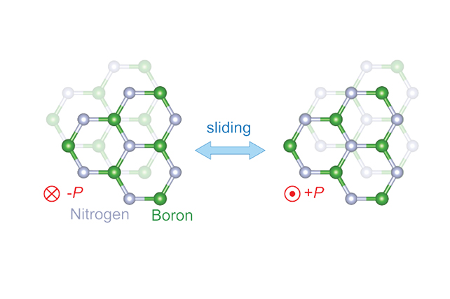
The transistor is made from a recently invented ultrathin ferroelectric material (with positive and negative charges on different levels) based on boron nitride. Two layers of the material are used, which shift slightly when electricity is applied, changing the configuration of the boron and nitrogen atoms.
This design makes the transistors incredibly fast and incredibly thin, two properties that can make a huge difference in making electronics more compact and more efficient. Think about being able to pack more storage and processing power in much smaller devices that use much less power.
What’s more, the slight shift in layers changes the properties of the material too, so there’s minimal wear or tear. The transistor is capable of toggling on and off at least 100 billion times with no sign of wear and tear, which means it’s far more long-lasting than the flash memory storage devices currently in use.
“Each time you write and erase a flash memory, you get some degradation,” says physicist Raymond Ashoori, from MIT.
“Over time, it wears out, which means that you have to use some very sophisticated methods for distributing where you’re reading and writing on the chip.”
The researchers behind the invention admit there’s a long way to go before these transistors can be used in real devices. Creating one device in a lab is a good start – but billions and billions of transistors are needed for the electronics of today.
However, the team is excited about where this can go next. It might also prove useful in exploring other physics fields, such as using light rather than electricity could to trigger the layer shift.
What’s clear is our current reliance on technology and digital devices means any innovations in this field could have far-reaching consequences and benefits that affect most people on the planet.
“When I think of my whole career in physics, this is the work that I think 10 to 20 years from now could change the world,” says Ashoori.
The research has been published in Science.
