Products You May Like
Scientists have succeeded in combining two exciting material types together for the very first time: an ultrathin semiconductor just a single atom thick; and a superconductor, capable of conducting electricity with zero resistance.
Both these materials have unusual and fascinating properties, and by putting them together through a delicate lab fabrication process, the team behind the research is hoping to open up all kinds of new applications in classical and quantum physics.
Semiconductors are key to the electrical gadgets that dominate our lives, from TVs to phones. What makes them so useful as opposed to regular metals is their electrical conductivity can be adjusted by applying a voltage to them (among other methods), making it easy to switch a current flow on and off.
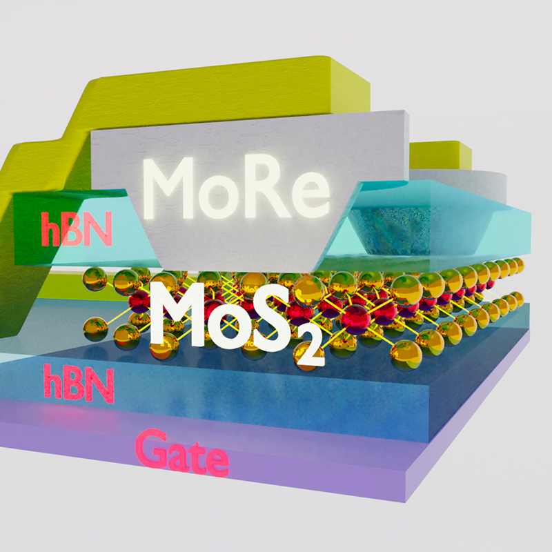
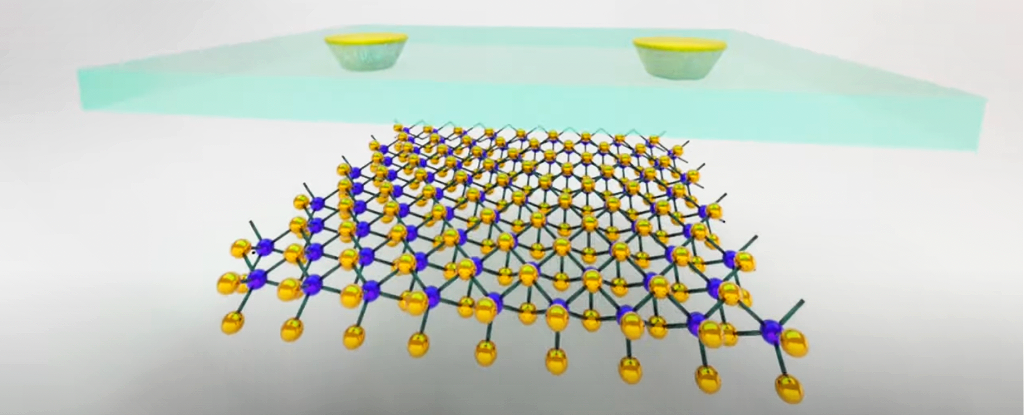
Here, a single layer of the semiconductor molybdenum disulfide (MoS2) was extracted and added to the fabrication process.
 (Mehdi Ramezani/Swiss Nanoscience Institute/University of Basel)
Then we have superconductors – able to transfer an electrical charge with perfect efficiency and nothing lost to heat, when at a certain temperature (usually an extremely low one).
In this setup, a superconductor called molybdenum rhenium (MoRe) was added to the device, and the researchers are expecting to observe completely new physical phenomena from their combined materials.
“In a superconductor, the electrons arrange themselves into pairs, like partners in a dance – with weird and wonderful consequences, such as the flow of the electrical current without a resistance,” says physicist Andreas Baumgartner, from the University of Basel in Switzerland.
“In the semiconductor molybdenum disulfide, on the other hand, the electrons perform a completely different dance, a strange solo routine that also incorporates their magnetic moments. Now we would like to find out which new and exotic dances the electrons agree upon if we combine these materials.”
Ultrathin semiconductors like the one used here are currently a hot investigation topic for researchers: they can be stacked together to form entirely new synthetic materials known as van der Waals heterostructures.
These structures have a lot of potentially innovative uses, such as being able to control electron magnetism with electric fields. However, a lot of this potential is still theoretical, because scientists just don’t know what effects they’re going to get yet and what devices they might be able to make. Which is why succeeding in creating this latest combination is so important.
In this latest setup, the team found evidence of strong coupling (interactions known as the proximity effect) between the semiconductor layer and the superconductor, when the materials were cooled down to just above absolute zero (-273.15°C or -459.67°F).
“Strong coupling is a key element in the new and exciting physical phenomena that we expect to see in such van der Waals heterostructures, but were never able to demonstrate,” says physicist Mehdi Ramezani, from the University of Basel.
Getting this semiconductor-superconductor link together isn’t easy – as you would expect, considering no one has done it before. The semiconductor is placed in a sandwich, with insulating layers above and below, while holes etched in the top of the insulating layer provide the electrical contact access.
The superconducting material fills the gaps left by the holes, and the process is finished inside a nitrogen-filled glove box to protect the finished system from damage. Remote-controlled micromanipulators are used to complete the fabrication, under an optical microscope.
With the fabrication now achieved, the testing and the experiments can begin – and have already started, in refrigerators cooled close to absolute zero. What’s more, the researchers think that they can use the same technique to work with other semiconductors in the future, further expanding its potential.
“Our measurements show that these hybrid monolayer semiconductor components are indeed possible – perhaps even with other, more exotic contact materials that would pave the way for further insights,” says Baumgartner.
The research has been published in Nano Letters.
